

Introduction
Designing a PCB with pogo pin connectors has become a critical part of modern electronics manufacturing, especially in Europe, where precision engineering, automation, and high-reliability standards are essential. Pogo pins, also known as spring-loaded connectors, are widely used for temporary electrical connections in testing, programming, and charging systems.
Whether you are designing IoT devices, medical electronics, automotive control boards, or industrial systems, understanding how to properly integrate pogo pin connectors into PCB design ensures durability, accuracy, and long-term performance.
In this guide, you will learn everything about how to design PCBs with pogo pin connectors, including layout techniques, spacing rules, material selection, mechanical alignment, and industry best practices tailored for the European electronics market.
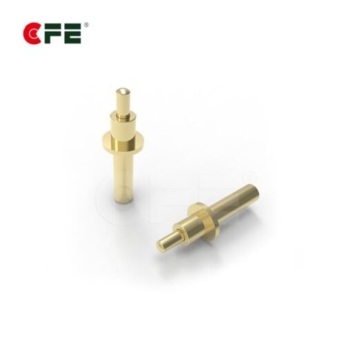
What Are Pogo Pin Connectors?
Pogo pin connectors are spring-loaded electrical contacts that provide a temporary but highly reliable connection between two electronic components. They consist of:
- A plunger (moving tip)
- A barrel (housing)
- A spring (internal mechanism)
When pressure is applied, the pin compresses and creates a stable electrical connection.
Key Advantages in PCB Design
- High durability (100,000+ cycles)
- Reliable signal transfer
- No soldering required for temporary contact
- Ideal for automated testing systems
- Perfect for compact PCB layouts
In Europe, pogo pin connectors are widely used in automotive testing systems in Germany, industrial automation in Italy, and medical devices in Switzerland.
Why Use Pogo Pin Connectors in PCB Design?
When designing PCBs, pogo pins offer several advantages over traditional connectors:
1. Fast Testing and Programming
Manufacturers use pogo pins in bed-of-nails test fixtures to quickly test PCB functionality without permanent soldering.
2. Space Saving Design
No bulky connectors are required, making them ideal for compact PCB layouts.
3. High Reliability
Spring-loaded contacts ensure stable connections even under vibration, which is crucial for automotive and aerospace applications in Europe.
4. Cost Efficiency
Reduces manual soldering and assembly time in mass production.
Step-by-Step Guide: How to Design PCB with Pogo Pin Connectors
Step 1: Define Application Requirements
Before starting PCB layout, determine:
- Signal type (power, data, RF)
- Current rating per pin
- Number of cycles required
- Environmental conditions (temperature, vibration)
European industries often follow strict IEC and ISO standards, especially in the automotive and medical sectors.
Step 2: Choose the Right Pogo Pin Type
There are different types of pogo pins:
- Standard signal pins
- High current pogo pins
- RF pogo pins
- Double-ended pogo pins
For PCB design in Europe-based applications, always choose RoHS-compliant and lead-free pogo pins.
Step 3: PCB Pad Design
The pad design is the most critical part.
Best practices:
- Use gold-plated pads (ENIG finish recommended)
- Maintain uniform pad diameter
- Avoid solder mask on contact areas
- Ensure flat and smooth surfaces
Recommended pad diameter:
- Small signal: 1.0 mm – 1.5 mm
- Power applications: 2.0 mm – 3.0 mm
Step 4: Spacing and Alignment
Correct spacing ensures proper contact and prevents wear.
- Minimum spacing: 1.27 mm (standard pitch)
- High precision applications: 0.5 mm–1.0 mm pitch
- Use alignment pins for mechanical accuracy
In European automation systems, CNC-guided alignment fixtures are commonly used for precision.
Step 5: Mechanical Design Considerations
Pogo pins require mechanical force to function properly.
Key factors:
- Compression height (stroke length)
- Contact force (typically 20g–100g per pin)
- Housing stability
- Anti-vibration design
Always ensure that PCB thickness supports mechanical pressure without bending.
Step 6: Signal Integrity Optimization
For high-speed signals:
- Keep trace lengths short
- Use controlled impedance routing
- Minimize via usage
- Separate power and signal pins
This is especially important in European telecom and automotive radar systems.
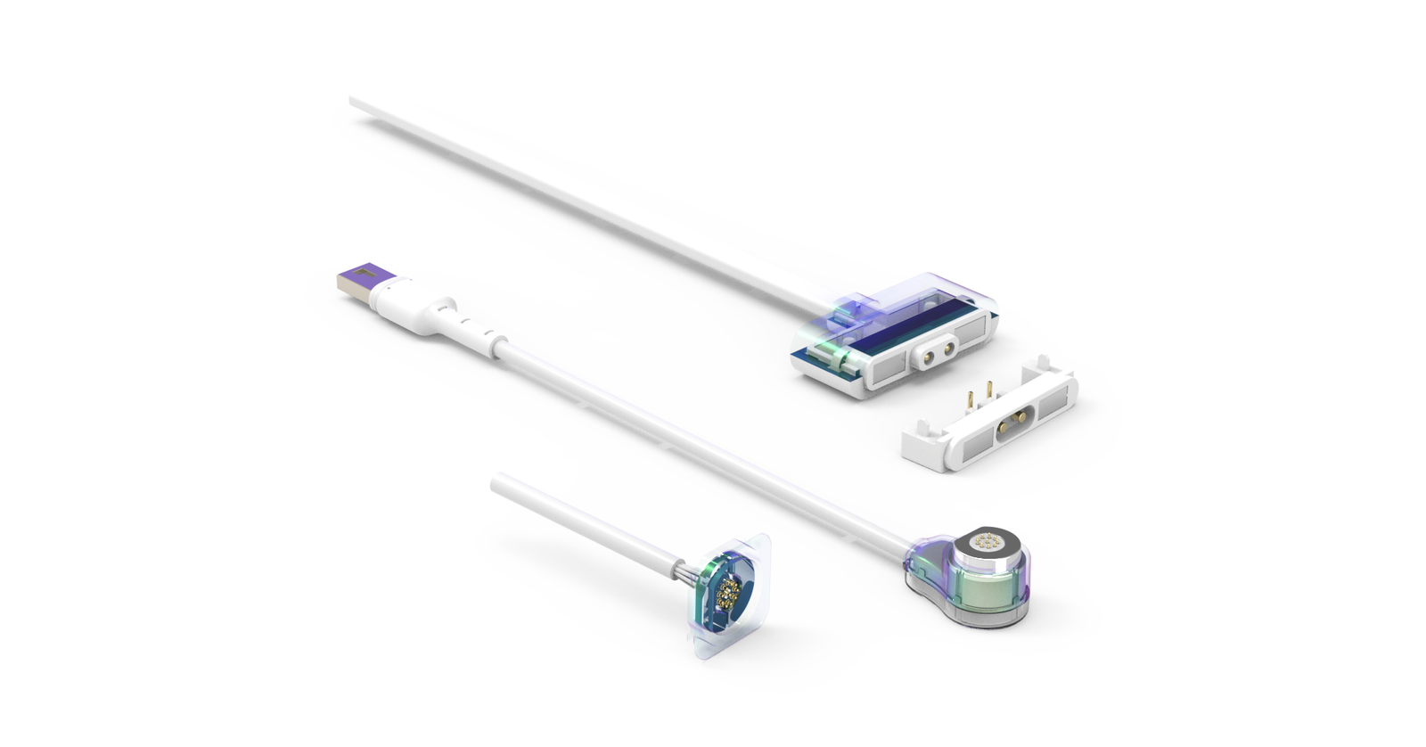
Step 7: Testing Fixture Integration
Most pogo pin PCBs are used in test fixtures.
Common applications:
- Automated PCB testing (ATE systems)
- Battery charging docks
- Firmware programming stations
Ensure repeatable alignment for mass production environments.
Step 8: Material Selection
Best materials for pogo pin PCB design:
- FR4 (standard PCB material)
- High TG FR4 (for high temperature)
- Copper thickness: 1 oz to 2 oz
- ENIG surface finish for durability
Common Applications in Europe
Pogo pin PCB designs are widely used in:
- Automotive ECUs (Germany, France)
- Medical devices (Switzerland, Netherlands)
- Industrial automation systems (Italy, Poland)
- Consumer electronics charging docks
- IoT smart devices
Common Mistakes to Avoid
- Incorrect pad sizing
- Poor alignment mechanism
- Using low-quality plating
- Ignoring mechanical stress
- Wrong spring force selection
Future Trends in Pogo Pin PCB Design
The European electronics industry is moving toward:
- Miniaturized pogo pin arrays
- High-density interconnect systems
- Smart test fixtures with AI diagnostics
- Magnetic + pogo hybrid connectors
FAQs
1. What is the main purpose of pogo pin connectors in PCB design?
Pogo pins are used for temporary electrical connections, mainly for testing, programming, and charging without soldering.
2. Are pogo pin connectors reliable for long-term use?
Yes, high-quality pogo pins can last over 100,000 cycles if properly designed and maintained.
3. What surface finish is best for pogo pin PCBs?
ENIG (Electroless Nickel Immersion Gold) is the most recommended finish for durability and conductivity.
4. Can pogo pins handle high current applications?
Yes, but you must use high-current-rated pogo pins and design thicker PCB traces accordingly.
5. Where are pogo pin PCBs commonly used in Europe?
They are widely used in automotive testing, medical electronics, industrial automation, and IoT devices.
Conclusion
Designing a PCB with pogo pin connectors requires careful attention to electrical, mechanical, and material considerations. In Europe-based industries, where precision and reliability are essential, pogo pins offer an efficient and cost-effective solution for testing and temporary connections.
By following proper pad design, spacing rules, and mechanical alignment techniques, engineers can achieve highly reliable PCB systems that meet modern industrial standards.
